| |
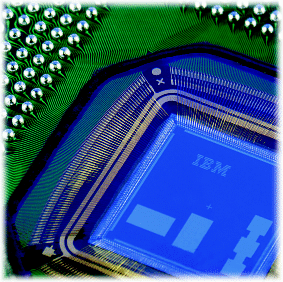
Howard's career with IBM

1998 - 1999
Began work as a regular full-time employee in IBM's Network Hardware Division in Research Triangle Park, North Carolina. Assigned to do verification work for a chip code-named Rainier, designed to be used in high-end IP switches. By the summer of 1999, it was becoming obvious that IBM was getting out of the IP-Ethernet hardware business.
1999 - 2000
Transferred to IBM's Server Group in Poughkeepsie, New York, where I helped bring up a switched fabric for POWER processor nodes, a component of the ASCI White supercomputer delivered to Lawrence Livermore National Laboratory in 2000 ( fastest computer in the world through 2001) and integral to IBM's commercial pSeries servers (pSeries line rebranded from RS/6000 in 2000, and rebranded again to Power Systems in 2008).
2000 - 2001
Began high-level design and logic entry for a pair of first-generation Infiniband chips, code-named Lexington and Concord. However, business plans changed (as they do when the Internet bubble bursts) and PCI Express emerges as the follow-on to PCI-X (instead of Infiniband).
2001 - 2004
The Server Group became the IBM Systems & Technology Group, and I delivered a piece of new chip code-named Eden, an I/O chip for the z990 eServer machine (zSeries line rebranded from System/390, starting with the z900). Eden allowed a standard off-the-shelf PCI Express card to communicate with IBM's proprietary self-timed interconnect (STI) with the mainframe's memory.
2004 - 2008
Found myself responsible for the Ethernet Data Router logic, a large portion of an ASIC code-named Thumper which was the follow-on to Eden. Large portions of functionality formerly provided by firmware running on embedded PPC processors was offloaded to custom logic in hardware, and the chip provided network virtualization for standard off-the-shelf 10Gbps Ethernet cards. Thumper shipped with IBM's System z9 and z10 mainframes.
2008 - 2010
Worked remotely with an IBM Storage team in Rochester, Minnesota on an FPGA-based RAID controller for enterprise-class SSDs, delivering an interface layer to Altera's PCI Express hard IP. Discovered I could work for extended periods of time from my parents' home in Arizona just as well as I could work from my office in New York, just as our teams now consist of IBMers located all across the globe.
2009 - 2010
Thumper 2 was a minor re-spin of the ASIC for the primary purpose of replacing IBM's STI with the industry-standard PCI Express interface. Though I was involved in the initial high-level design, other engineers were assigned to the actual implementation (as I was already committed to and otherwise occupied by work on the Rochester chip). I rejoined the effort after they froze the VHDL but was able to help fix some bugs via rewiring the gates (via ECOs ).
2010 - 2011
Joined the PCI Express team to develop a hybrid switch incorporating cores from IBM's Microelectronics division. The highly ambitious Shelby project was scrapped, followed by the streamlined Fiesta project, which was also canceled. Eventually did some preliminary high-level design work for a PTL (PCIe Transaction Layer) core before moving on to the next successful project.
2011 - 2013
Designed the PCIe Gen2 x8 interface logic, including a custom config space with SR-IOV support, for the CORSA Accelerator chip that is used to implement, among other things, IBM's zEDC (zEnterprise Data Compression) capability on the zEC12/zBC12 mainframes. Based on an Altera Stratix V GX FPGA mounted on a custom half-height board, CORSA provides a standard interface/wrapper for accelerating custom applications per customer requirements.
2012 - present
On the Kraken networking/storage ASIC with sidecare FPGA, I find myself owning all the legacy Ethernet Data Router logic brought forward from Thumper 2, plus additional blocks of logic including the QMgr+PBB (dynamically-configurable queue manager with embedded DRAM interface/controller) and a new physical interface for ASIC-FPGA communication. In addition to logic design, I'm also responsible for ensuring correctly-designed async crossings across clock domains throughout the chip and TLI/FEP (insertion of test logic and front-end processing for PD).
|
|